| CPC B81B 7/0006 (2013.01) [B81C 1/00301 (2013.01)] | 11 Claims |
|
1. An electrical interconnection structure, used to provide electrical connections between electronic devices and external circuits, the electronic devices located inside an electronic apparatus and includes a Micro Electro Mechanical Systems (MEMS) device; the electronic apparatus further comprising a base, the MEMS device is located in a cavity at a side of the base; the electrical interconnection structure is located at a side of the cavity facing away from the base; an orthographic projection of the electrical interconnection structure to the base does not overlap with an orthographic projection of the MEMS device to the base; an orthographic projection of the electrical interconnection structure along a thickness direction perpendicular to the electronic apparatus does not overlap with an orthographic projection of the MEMS device along the thickness direction perpendicular to the electronic apparatus; the electronic apparatus also comprises a sacrificial layer deposited on the base, and the cavity is formed in the sacrificial layer; the electrical interconnection structure comprising:
a bonding metal located at a side of the sacrificial layer away from the base; an orthographic projection of the bonding metal to the base does not overlap with the cavity;
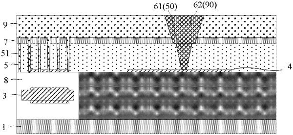
a first dielectric layer located at a side of the bonding metal, wherein the first dielectric layer comprises a first through hole penetrating the first dielectric layer, and the first through hole only penetrates the first dielectric layer; the first through hole exposes the bonding metal, and the first through hole is filled with a first conductive material electrically connected to the bonding metal; and
a second dielectric layer located at a side of the first dielectric layer facing away from the bonding metal, wherein the second dielectric layer comprises a second through hole, the second dielectric layer comprises a first dielectric sub-layer and a second dielectric sub-layer that are stacked, and the first dielectric sub-layer is located between the second dielectric sub-layer and the first dielectric layer; the second through hole completely penetrates the first dielectric sub-layer and the second dielectric sub-layer; an orthographic projection of a second conductive material filed in the second through hole onto a plane of the bonding metal completely covers an orthographic projection of the first conductive material filed in the first through hole onto the plane of the bonding metal, and the second conductive material is electrically connected to the first conductive material; and a gap is formed in the first conductive material and/or the second conductive material.
|