| CPC B24B 37/26 (2013.01) [B24B 37/24 (2013.01); B24B 53/017 (2013.01); H01L 21/31055 (2013.01); H01L 21/3212 (2013.01); H01L 21/7684 (2013.01); H01L 21/76805 (2013.01); H01L 21/76819 (2013.01); H01L 21/76895 (2013.01); H01L 23/53257 (2013.01)] | 16 Claims |
|
1. A method of fabricating a semiconductor device, comprising:
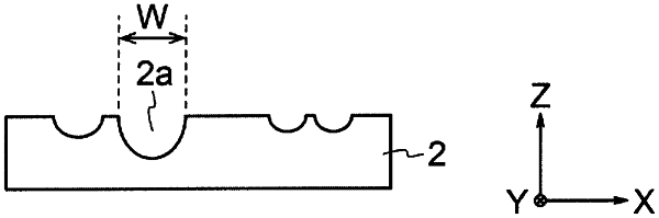
providing a polishing pad with a surface that has plural recess portions, wherein an average width of the recess portions at one area of the surface in a direction parallel to the surface is 20 μm or less, and an average density of the recess portions at one area of the surface is 1,300/mm2 or more;
after providing the polishing pad, holding the polishing pad on a pad polishing table;
after holding the polishing pad, supplying a polishing liquid to the surface of the polishing pad;
after supplying the polishing liquid, polishing a substrate using the polishing liquid in a gap between the polishing pad that includes the surface having the plural recess portions and the substrate; and
after polishing the substrate, dressing an upper surface of the polishing pad that includes the surface having the plural recess portion using a dresser.
|