| CPC A61B 10/0064 (2013.01) [A61B 5/1477 (2013.01); A61B 5/14517 (2013.01); A61B 5/4266 (2013.01); A61B 5/6833 (2013.01); B23K 1/008 (2013.01); B23K 1/0016 (2013.01); B23K 26/38 (2013.01); B23K 26/384 (2015.10); B23K 26/389 (2015.10); B23K 26/402 (2013.01); B29C 69/00 (2013.01); G01N 33/48707 (2013.01); A61B 2562/0295 (2013.01); A61B 2562/12 (2013.01); A61B 2562/125 (2013.01); A61B 2562/164 (2013.01); A61B 2562/166 (2013.01); B23K 2101/36 (2018.08); B23K 2101/42 (2018.08); B23K 2103/172 (2018.08); B23K 2103/42 (2018.08); B29K 2027/06 (2013.01); B29K 2995/0005 (2013.01); B29L 2009/008 (2013.01); B29L 2031/34 (2013.01); B29L 2031/753 (2013.01); H05K 1/16 (2013.01); H05K 2201/10151 (2013.01)] | 16 Claims |

|
1. A method of fabrication for a biological fluid sensor for analyzing at least one analyte in human biological fluid, said biological fluid sensor comprising electronic components, electrochemical components, and chemical components, the method comprising:
fabricating at least one substrate;
fabricating at least one circuit on the at least one substrate;
placing the electronic components onto the at least one circuit, wherein the electronic components include at least one microcontroller and at least one transceiver;
fabricating at least two electrodes, wherein the at least two electrodes are comprised of at least one active electrode and at least one reference electrode;
applying an ionophore coating on the at least one active electrode;
sealing the at least one active electrode to create an electronic layer; and
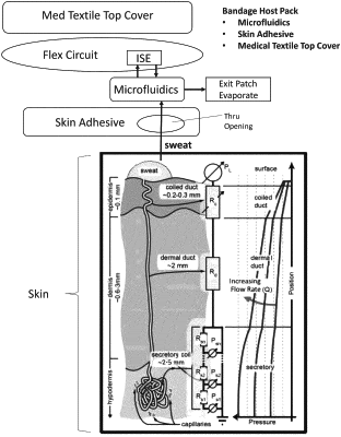
integrating the electronic layer with a top cover layer, a microfluidic management layer, and a double-sided adhesive layer;
wherein the step of fabricating the at least two electrodes further comprises:
fabricating a metallization paste;
constructing the at least one reference electrode by applying the metallization paste on top of at least one first trace metal of the at least one circuit and annealing; and
constructing the at least one active electrode by applying the metallization paste on top of at least one second trace metal of the at least one circuit and annealing;
forming a conductive trace in a first ring around the at least one active electrode, wherein the conductive trace in the first ring around the at least one active electrode does not contact the at least one active electrode;
forming a second ring around the at least one active electrode, wherein the second ring around the at least one active electrode is inside the first ring around the at least one active electrode, and wherein the first ring around the at least one active electrode does not contact the second ring around the at least one active electrode; and
applying the ionophore coating on the at least one active electrode such that the ionophore coating completely covers the at least one active electrode and is contained within the second ring;
wherein the step of integrating the electronic layer with the top cover layer, the microfluidic management layer, and the double-sided adhesive layer further comprises:
placing the electronic layer on top of an adhesive side of the top cover layer;
surrounding the at least two electrodes with the microfluidic management layer;
placing a double-sided adhesive layer on top of the electronic layer such that the double-sided adhesive layer covers the electronic layer; and
pressing the top cover layer, the microfluidic management layer, the electronic layer, and the double-sided adhesive layer.
|