US 11,882,772 B2
Conductive-bridging semiconductor memory device formed by selective deposition
Kangguo Cheng, Schenectady, NY (US); Chanro Park, Clifton Park, NY (US); Julien Frougier, Albany, NY (US); and Ruilong Xie, Niskayuna, NY (US)
Assigned to International Business Machines Corporation, Armonk, NY (US)
Filed by International Business Machines Corporation, Armonk, NY (US)
Filed on Aug. 30, 2021, as Appl. No. 17/460,504.
Prior Publication US 2023/0068851 A1, Mar. 2, 2023
Int. Cl. H10N 70/00 (2023.01); H10B 63/00 (2023.01); H10N 70/20 (2023.01)
CPC H10N 70/011 (2023.02) [H10B 63/00 (2023.02); H10N 70/245 (2023.02); H10N 70/8416 (2023.02)] 17 Claims
OG exemplary drawing
 
1. A method of forming a memory cell, comprising:
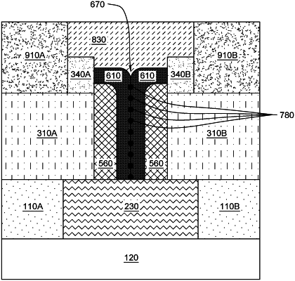
forming a seam in a via located on top of a bottom electrode based on pinching off the via, wherein pinching off the via includes selectively depositing a dielectric material on top of a dielectric spacer formed on a sidewall of the via, and further wherein pinching off the via results in the seam being in direct contact with the bottom electrode.