| CPC H10N 60/0912 (2023.02) [H10N 60/0884 (2023.02); H10N 60/805 (2023.02); H10N 60/0241 (2023.02)] | 18 Claims |

|
1. A method for fabricating a device structure, comprising:
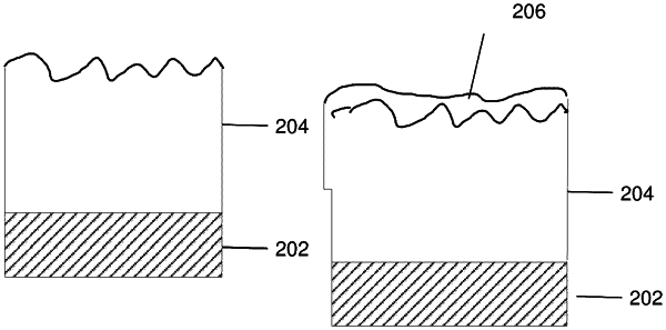
depositing a layer of a first material comprising metal atom species on a selected surface of a device layer;
depositing a layer of a second material on a surface of the layer of first material; and performing plasma etching on the layer of second material and the layer of first material to form an etched surface of the layer of first material wherein the etched surface of the layer of first material is smoother than the initially deposited surface of the layer of first material deposited on the selected surface of the device layer, wherein the smoother layer of the first material after the plasma etching has lower surface roughness than the initially deposited surface of the layer of first material on the selected surface of the device layer, wherein the plasma etching process employs at least one of: an argon/chlorine mixture (Ar/Cl2), an argon/boron trichloride mixture (Ar/BCl3), or either one of the Ar/Cl2 or the Ar/BCl3 with the addition of a nitrogen (N2) diluent gas.
|