| CPC H10K 71/621 (2023.02) [H10K 59/12 (2023.02); H10K 85/40 (2023.02); H10K 50/844 (2023.02); H10K 59/1201 (2023.02); H10K 71/00 (2023.02)] | 17 Claims |
|
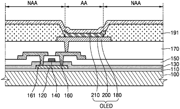
1. A method of manufacturing a display apparatus, the method comprising:
forming a conductive layer on a substrate;
forming a preliminary insulating pattern on the conductive layer;
forming an insulating pattern by developing with a first solution; and
treating the insulating pattern with a second solution, wherein
the preliminary insulating pattern comprises a first material, the first material being a siloxane-based alkali soluble polymer,
the first solution comprises a nitrogen compound,
the second solution comprises HF,
the first material is different from the nitrogen compound,
the insulating pattern comprises a first region and a second region,
the second region is between the conductive layer and the first region, and
the concentration of the nitrogen compound is reduced from the first region to the second region.
|