| CPC H10K 59/38 (2023.02) [H10K 50/865 (2023.02); H10K 59/122 (2023.02); H10K 71/00 (2023.02); H10K 59/1201 (2023.02); H10K 2102/331 (2023.02)] | 22 Claims |
|
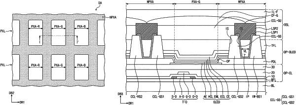
1. A display panel, comprising:
an emission element which outputs a source light and includes a first electrode, an emission layer disposed on the first electrode, and a second electrode disposed on the emission layer;
a pixel definition layer, in which an opening exposing at least a portion of the first electrode is defined;
a first light-conversion pattern disposed on the pixel definition layer;
a first light-blocking pattern disposed on an outer side of the first light-conversion pattern in a plan view; and
a second light-conversion pattern disposed on the emission element and which overlaps with the emission element in the plan view, wherein the first and second light-conversion patterns are spaced apart from each other or forming an interface therebetween.
|