| CPC H10K 59/1315 (2023.02) [G09G 3/2096 (2013.01); G09G 3/3266 (2013.01); G11C 19/28 (2013.01); G09G 2300/0426 (2013.01); G09G 2310/0286 (2013.01); G09G 2310/0291 (2013.01); G09G 2330/021 (2013.01); H10K 59/124 (2023.02)] | 20 Claims |
|
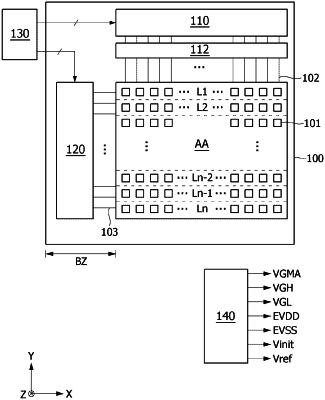
1. A display panel comprising:
a circuit layer disposed on a substrate and including a plurality of transistors;
a light emitting element layer disposed on the circuit layer and including a plurality of light emitting elements; and
an encapsulation layer on the light emitting element layer,
wherein the circuit layer includes a first transistor and a second transistor,
wherein the first transistor includes:
a first oxide semiconductor pattern,
a gate electrode overlapping the first oxide semiconductor pattern above the first oxide semiconductor pattern,
a first electrode in contact with one side of the first oxide semiconductor pattern on the first oxide semiconductor pattern, and
a second electrode in contact with the other side of the first oxide semiconductor pattern on the first oxide semiconductor pattern, and
wherein the second transistor includes:
a second oxide semiconductor pattern,
a gate electrode overlapping the second oxide semiconductor pattern above the second oxide semiconductor pattern,
a first electrode in contact with one side of the second oxide semiconductor pattern, and
a second electrode in contact with the other side of the second oxide semiconductor pattern,
wherein the circuit layer includes a first-first metal pattern disposed on the substrate to overlap the first oxide semiconductor pattern, a first-second metal pattern disposed on the substrate to overlap the second oxide semiconductor pattern, and a second metal pattern disposed between the second oxide semiconductor pattern and the first-second metal pattern,
wherein the first and second electrodes of the first transistor do not overlap with the first-second metal pattern from a cross-sectional view,
wherein the second electrode of the first transistor extends toward the substrate and contacts the first-first metal pattern.
|