| CPC H10K 59/131 (2023.02) [G09G 3/3266 (2013.01); G09G 3/3275 (2013.01); H10K 50/844 (2023.02); H10K 71/00 (2023.02); H10K 2102/00 (2023.02)] | 17 Claims |
|
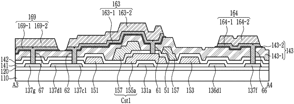
1. A display device, comprising:
a substrate;
an active layer disposed on the substrate;
a first conductive layer including a driving gate electrode and a scan line extending in a first direction;
a second conductive layer including a storage line;
a third conductive layer including a first connecting member disposed above the storage line;
an insulating layer disposed between the storage line and the first connecting member and including a first sub-insulating layer disposed on the second conductive layer and a second sub-insulating layer disposed under the third conductive layer; and
a data line and a driving voltage line each crossing the scan line and extending in a second direction, wherein
the first connecting member electrically connects the driving gate electrode and the active layer, and
an edge of the second sub-insulating layer is disposed outside of an edge of the third conductive layer in a plan view.
|