| CPC H10K 59/131 (2023.02) [H10K 50/844 (2023.02); H10K 50/8426 (2023.02); H10K 59/38 (2023.02)] | 20 Claims |
|
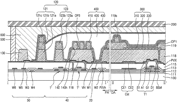
1. A display device comprising:
a substrate including a display area configured for displaying an image and a peripheral area positioned outside of the display area;
a first thin film transistor disposed on the display area;
a display element electrically connected to the first thin film transistor, the display element comprising a pixel electrode, an intermediate layer, and an opposite electrode;
a driving circuit portion disposed on the peripheral area, the driving circuit portion comprising a second thin film transistor;
a dam portion disposed in the peripheral area, the dam portion protruding from the substrate; and
a thin-film encapsulation layer covering the display element, the thin-film encapsulation layer comprising at least one inorganic encapsulation layer and at least one organic encapsulation layer,
wherein the dam portion at least partially overlaps the driving circuit portion, and
wherein the thin-film encapsulation layer at least partially overlaps the driving circuit portion.
|