| CPC H10B 20/20 (2023.02) [G11C 17/146 (2013.01); G11C 17/16 (2013.01); G11C 17/18 (2013.01)] | 8 Claims |
|
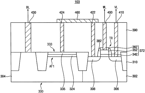
1. A one-time programmable (OTP) memory device, comprising:
an access transistor including:
a gate structure on a substrate; and
first and second impurity regions at respective portions of the substrate adjacent to the gate structure;
a word line electrically connected to the gate structure;
a voltage line directly connected to the first impurity region;
a first well at an upper portion of the substrate, the first well being doped with impurities having a first conductivity type;
a first filling oxide layer on the first well;
a first semiconductor layer on the first filling oxide layer, the first semiconductor layer being doped with impurities having the first conductivity type and electrically connected to the second impurity region; and
a bit line electrically connected to the first well.
|