| CPC H05K 3/3447 (2013.01) [H05K 1/115 (2013.01); H05K 1/184 (2013.01); H05K 3/306 (2013.01)] | 18 Claims |
|
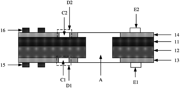
1. A printed circuit board, wherein a plurality of target holes penetrate through the printed circuit board, and wherein the printed circuit board comprises a plurality of blocks disposed in a first area, the first area comprises at least one side of the printed circuit board and is adjacent to the plurality of target holes but does not include the plurality of target holes, wherein each block of the plurality of blocks is next to a target hole of the plurality of target holes, and wherein the plurality of blocks are configured to block liquid flow; and
wherein:
the printed circuit board comprises a first solder resist layer, a base material over the first solder resist layer, a conductive pattern layer over the base material, and a second solder resist layer over the conductive pattern layer;
the target holes penetrate through the first solder resist layer, the base material, the conductive pattern layer, and the second solder resist layer; and
the blocks of the plurality of blocks each comprise at least one of a groove or a protrusion;
for each block of the plurality of blocks that comprises a groove, the respective groove is physically separate from the conductive pattern layer;
when the first area comprises a side of the printed circuit board on which the first solder resist layer is located, and the plurality of blocks comprises a first groove, the first groove is defined by a first auxiliary hole that penetrates through the first solder resist layer to a surface of the base material; and
when the first area comprises a side of the printed circuit board on which the second solder resist later is located, and the plurality of blocks comprises a second groove, the second groove is defined by a second auxiliary hole that penetrates through the second solder resist layer to a surface of the base material.
|