| CPC H03M 3/376 (2013.01) [G01C 19/5649 (2013.01); G01C 19/5712 (2013.01); G01C 19/5776 (2013.01); G01P 1/00 (2013.01); G01P 15/08 (2013.01); H03F 3/45 (2013.01); H03M 3/34 (2013.01); H03M 3/458 (2013.01); H03M 3/464 (2013.01); H03F 2203/45151 (2013.01); H03F 2203/45546 (2013.01)] | 20 Claims |
|
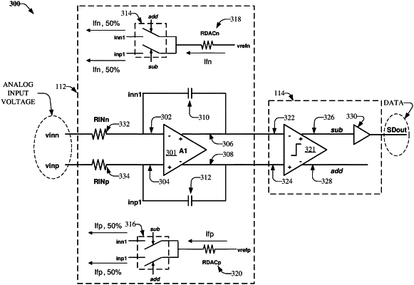
1. A sigma-delta analog-to-digital converter (ADC), comprising:
a differential amplifier comprising respective differential amplifier inputs and respective differential amplifier outputs, wherein the respective differential amplifier outputs are electrically coupled, via respective capacitances, to the respective differential amplifier inputs, wherein the respective differential amplifier inputs are electrically coupled, based on a pair of switch control signals via respective pairs of electronic switches, to respective feedback resistances, wherein a first feedback resistance of the respective feedback resistances is electrically coupled to a first defined reference voltage, wherein a second feedback resistance of the respective feedback resistances is electrically coupled to a second defined reference voltage that is different from the first defined reference voltage, wherein the sigma-delta ADC minimizes bias instability corresponding to a flicker noise that has been injected into the respective differential amplifier inputs via variations in respective values of the first feedback resistance and the second feedback resistance of the respective, and wherein the flicker noise has been injected into the respective differential amplifier inputs in response to a reference voltage average of the first defined reference voltage and the second defined reference voltage being different from an input voltage average of respective input voltages that have been applied to the respective differential amplifier inputs; and
a differential comparator comprising differential comparator inputs and complementary comparator outputs, wherein the complementary comparator outputs comprise the pair of switch control signals.
|