| CPC H03K 5/1565 (2013.01) [H03K 5/134 (2014.07); H03K 19/20 (2013.01); H03K 2005/00195 (2013.01)] | 39 Claims |
|
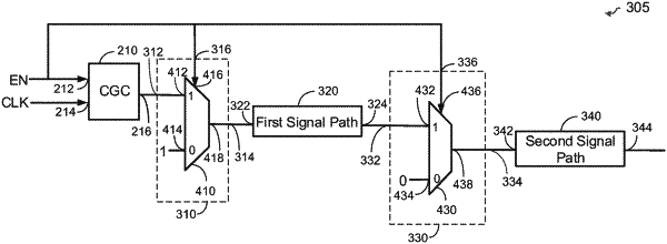
1. A system, comprising:
a first park circuit having a signal input, an output, and a control input, wherein the first park circuit is configured to couple the signal input of the first park circuit to the output of the first park circuit or to park the output of the first park circuit at a first logic value in response to a first control signal;
a first signal path having an input and an output, wherein the input of the first signal path is coupled to the output of the first park circuit;
a second park circuit having a signal input, an output, and a control input, wherein the signal input of the second park circuit is coupled to the output of the first signal path, wherein the second park circuit is configured to couple the signal input of the second park circuit to the output of the second park circuit or to park the output of the second park circuit at a second logic value in response to a second control signal; and
a second signal path having an input and an output, wherein the input of the second signal path is coupled to the output of the second park circuit.
|