| CPC H02J 50/20 (2016.02) [H02J 50/005 (2020.01); H02J 50/10 (2016.02); H04B 5/0037 (2013.01)] | 14 Claims |
|
1. An electronic device comprising:
a housing;
wireless charging circuitry disposed in the interior of the housing; and
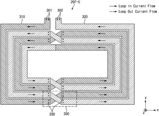
a wireless charging antenna having a spiral shape and electrically connected to the wireless charging circuitry,
wherein the wireless charging antenna includes:
a first conductive pattern corresponding to an area where current spirally flows toward the inside of the wireless charging antenna, among areas configured to form the wireless charging antenna; and
a second conductive pattern corresponding to an area where the current spirally flows toward the outside of the wireless charging antenna, among the areas configured to form the wireless charging antenna, wherein the second conductive pattern is disposed parallel to the first conductive pattern on a side of the first conductive pattern on the same plane,
wherein the first conductive pattern and the second conductive pattern are formed of a plurality of layers including a first layer and a second layer, and
wherein in a first area where part of the first conductive pattern and part of the second conductive pattern intersect each other, the first conductive pattern does not include the first layer, and the second conductive pattern does not include the second layer.
|