| CPC H01L 33/62 (2013.01) [H01L 25/167 (2013.01); H01L 2933/0066 (2013.01)] | 8 Claims |
|
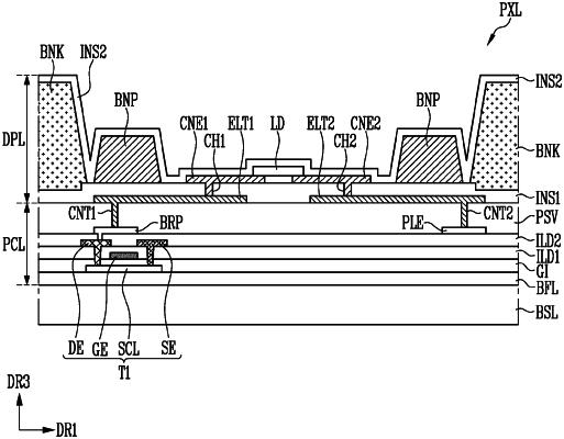
1. A display device comprising:
a substrate; and
a display element layer disposed on the substrate and including a light emitting element that emits light in a display direction, wherein
the display element layer includes:
a first contact electrode electrically connected to the light emitting element;
a second contact electrode electrically connected to the light emitting element; and
a bank pattern having a shape extending in the display direction,
the light emitting element is above at least a portion of both the first contact electrode and the second contract electrode, and
at least one of the first contact electrode, the second contact electrode, and the bank pattern includes a transparent conductive polymer.
|