| CPC H01L 33/54 (2013.01) [H01L 31/0203 (2013.01); H01L 31/02322 (2013.01); H01L 31/186 (2013.01); H01L 33/0095 (2013.01); H01L 33/502 (2013.01); H01L 21/568 (2013.01); H01L 33/486 (2013.01); H01L 33/505 (2013.01); H01L 33/56 (2013.01); H01L 2224/18 (2013.01); H01L 2224/24 (2013.01); H01L 2224/2518 (2013.01); H01L 2224/82 (2013.01); H01L 2933/005 (2013.01); H01L 2933/0033 (2013.01); H01L 2933/0041 (2013.01); H01L 2933/0058 (2013.01)] | 20 Claims |
|
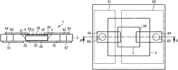
1. A method for producing a plurality of optoelectronic semiconductor devices comprising:
a) providing a plurality of semiconductor chips, which are spaced from one another in a lateral direction;
b) forming a package body assembly, which is arranged at least in part between the semiconductor chips;
c) forming a plurality of fillets, which each adjoin a semiconductor chip and which are delimited in the lateral direction by a side face of the respective semiconductor chip and the package body assembly, wherein forming the plurality of fillets is performed at least in part prior to forming the package body assembly, and wherein the fillets extend in each case around an entire circumference of the associated semiconductor chip, the fillets comprise a convex curvature when viewed from the radiation exit face, or both; and
d) singulating the package body assembly into a plurality of optoelectronic semiconductor devices, wherein each semiconductor device comprises at least one semiconductor chip and a part of the package body assembly as its package body and wherein the semiconductor chips are each free of package body material on a radiation exit face of the semiconductor device opposite a mounting surface.
|