| CPC H01L 29/0847 (2013.01) [H01L 29/1033 (2013.01); H01L 29/66553 (2013.01)] | 20 Claims |
|
1. A semiconductor device, comprising:
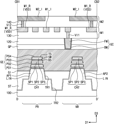
an active pattern on a substrate;
a source/drain pattern on the active pattern, the source/drain pattern including a bottom surface in contact with a top surface of the active pattern;
a channel pattern connected to the source/drain pattern;
a gate electrode extended to cross the channel pattern;
a fence insulating layer extended from a side surface of the active pattern to a lower side surface of the source/drain pattern; and
a pair of middle insulating patterns at both sides of the bottom surface of the source/drain pattern, the pair of middle insulating patterns being between the active pattern and the source/drain pattern in contact with an inner side surface of the fence insulating layer.
|