| CPC H01L 25/0657 (2013.01) [H01L 24/05 (2013.01); H01L 24/13 (2013.01); H01L 24/48 (2013.01); H01L 24/49 (2013.01); H01L 24/73 (2013.01); H01L 25/105 (2013.01); H01L 25/18 (2013.01); H01L 25/50 (2013.01); H01L 2224/02331 (2013.01); H01L 2224/02379 (2013.01); H01L 2224/02381 (2013.01); H01L 2224/0401 (2013.01); H01L 2224/13024 (2013.01); H01L 2224/48108 (2013.01); H01L 2224/48157 (2013.01); H01L 2224/49173 (2013.01); H01L 2224/73265 (2013.01); H01L 2225/0651 (2013.01); H01L 2225/06548 (2013.01); H01L 2225/06558 (2013.01); H01L 2225/06568 (2013.01); H01L 2225/06586 (2013.01); H01L 2225/1035 (2013.01); H01L 2225/1041 (2013.01); H01L 2225/1058 (2013.01)] | 20 Claims |
|
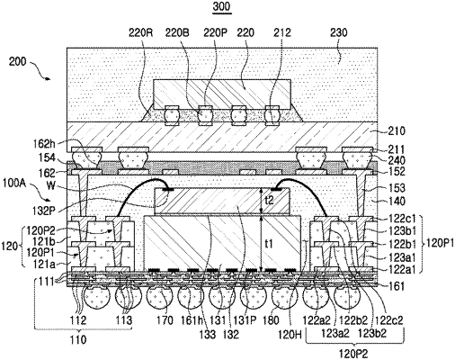
1. A semiconductor package, comprising:
a redistribution substrate including a first redistribution structure;
a first semiconductor chip disposed on the redistribution substrate, and including a first connection pad electrically connected to the first redistribution structure, the first connection pad being disposed on a lower surface of the first semiconductor chip;
a second semiconductor chip disposed on an upper surface of the first semiconductor chip and including a second connection pad disposed on an upper surface of the second semiconductor chip;
a vertical connection conductor disposed on the redistribution substrate, and adjacent to the first semiconductor chip and the second semiconductor chip, the vertical connection conductor being electrically connected to the first redistribution structure;
an encapsulant encapsulating at least a portion of the first semiconductor chip, the second semiconductor chip, and the vertical connection conductor; and
a conductive wire electrically connecting the second connection pad and a top of the vertical connection conductor,
wherein the upper surface of the second semiconductor chip is located on a level higher than the top of the vertical connection conductor.
|