| CPC H01L 23/5286 (2013.01) [H01L 21/76898 (2013.01); H01L 21/8221 (2013.01); H01L 23/481 (2013.01); H01L 27/0694 (2013.01); H01L 23/53209 (2013.01); H01L 23/53228 (2013.01); H01L 23/53242 (2013.01); H01L 23/53257 (2013.01)] | 8 Claims |
|
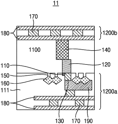
1. A semiconductor architecture comprising:
a carrier substrate;
a first semiconductor device provided on a first surface of the carrier substrate, the first semiconductor device being configured to route signals;
a second semiconductor device provided on a second surface of the carrier substrate opposite to the first surface of the carrier substrate, the second semiconductor device being configured to supply power; and
a buried power rail (BPR) included inside of the carrier substrate and extending from the first surface of the carrier substrate to the second surface of the carrier substrate, the BPR being configured to deliver the power from the second semiconductor device to the first semiconductor device,
wherein the second semiconductor device comprises power distribution network (PDN) metal lines.
|