US 11,881,447 B2
Package core assembly and fabrication methods
Han-Wen Chen, Cupertino, CA (US); Steven Verhaverbeke, San Francisco, CA (US); Giback Park, San Jose, CA (US); Kyuil Cho, Santa Clara, CA (US); Kurtis Leschkies, San Jose, CA (US); Roman Gouk, San Jose, CA (US); Chintan Buch, Santa Clara, CA (US); Vincent Dicaprio, Pleasanton, CA (US); Bernhard Stonas, Hayward, CA (US); and Jean Delmas, Santa Clara, CA (US)
Assigned to Applied Materials, Inc., Santa Clara, CA (US)
Filed by Applied Materials, Inc., Santa Clara, CA (US)
Filed on Apr. 12, 2021, as Appl. No. 17/227,867.
Application 17/227,867 is a continuation of application No. 16/886,704, filed on May 28, 2020.
Application 16/886,704 is a continuation in part of application No. 16/698,680, filed on Nov. 27, 2019.
Prior Publication US 2021/0249345 A1, Aug. 12, 2021
Int. Cl. H01L 23/538 (2006.01); H01L 23/367 (2006.01); H01L 23/498 (2006.01); H01L 21/48 (2006.01); H01L 23/14 (2006.01)
CPC H01L 23/49838 (2013.01) [H01L 21/486 (2013.01); H01L 23/147 (2013.01); H01L 23/49827 (2013.01); H01L 23/49866 (2013.01)] 18 Claims
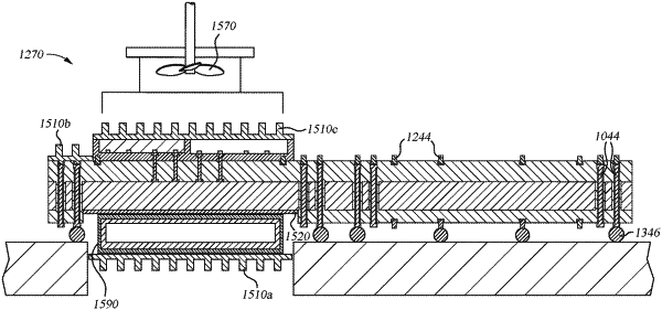
OG exemplary drawing
 
1. A semiconductor device assembly, comprising:
a silicon core structure comprising:
a first side opposing a second side; and
a conductive interconnection formed through the silicon core structure, wherein the conductive interconnection has a first surface exposed at the first side, a second surface exposed at the second side, and a third surface disposed between the first surface and the second surface;
an insulating layer disposed over the first side, the second side, and between the third surface of the conductive interconnection and the silicon core structure; and
a heat exchanger coupled to the silicon core structure, wherein the heat exchanger is disposed within a pocket formed in the insulating layer and coupled to the silicon core structure via an interfacial layer.