| CPC H01L 21/568 (2013.01) [H01L 21/561 (2013.01); H01L 21/78 (2013.01); H01L 23/3114 (2013.01); H01L 23/3121 (2013.01); H01L 23/3135 (2013.01); H01L 23/367 (2013.01); H01L 23/49838 (2013.01); H01L 23/528 (2013.01); H01L 24/19 (2013.01); H01L 24/96 (2013.01); H01L 25/0657 (2013.01); H01L 23/5389 (2013.01); H01L 2223/5448 (2013.01); H01L 2224/04105 (2013.01); H01L 2224/12105 (2013.01); H01L 2224/32225 (2013.01); H01L 2224/92144 (2013.01); H01L 2224/97 (2013.01); H01L 2924/19105 (2013.01)] | 9 Claims |
|
1. A method of packaging a chip, comprising:
providing a wafer prepared with a plurality of dies, the wafer includes front and back wafer surfaces, wherein the front wafer surface of the wafer is an active wafer surface with bond pads of the plurality of dies;
forming a protective layer on the front wafer surface, the protective layer being unitary and having first and second protective layer surfaces, wherein the second protective layer surface is disposed on the front wafer surface;
forming via openings in the protective layer to expose the bond pads, wherein the via openings comprises sidewalls not parallel to the front wafer surface;
dicing the wafer with the protective layer to separate the pluralities of dies into individual chips with front and back chip surfaces, wherein the front chip surface of the chips comprises the bond pads;
mounting the plurality of chips with the protective layer on a chip carrier with an adhesive layer, wherein the first protective layer surface is disposed on the adhesive layer;
encapsulating the plurality of chips with a high pressured encapsulant to form a mold panel, the mold panel includes first and second encapsulant surfaces of the high pressured encapsulant, wherein the first encapsulant surface is coplanar with the first protective layer surface;
detaching the chip carrier with the adhesive layer from the mold panel with the plurality of chips;
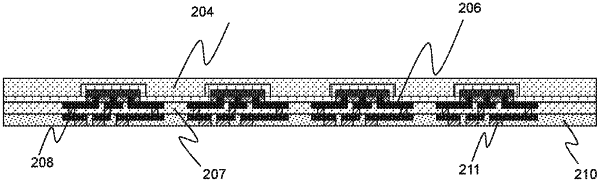
forming a rewiring structure on the first protective layer surface of the protective layer, wherein the rewiring structure includes conductive lines electrically coupled to the bond pads of the plurality of chips, and forming the rewiring structure comprises
forming first patterned rewiring lines of a first rewiring layer directly on the first protective layer surface, wherein the first patterned rewiring lines are connected to the bond pads by via contacts in the via openings, and
forming a first rewiring encapsulation layer, wherein the first rewiring encapsulation layer covers the first patterned rewiring lines; and
singulating the plurality of chips of the mold panel with the high pressured encapsulant and the rewiring structure to form a plurality of chip packages.
|