| CPC H01L 21/485 (2013.01) [C25D 1/003 (2013.01); C25D 5/10 (2013.01); C25D 5/22 (2013.01); H01L 21/4825 (2013.01); H01L 21/4882 (2013.01); B33Y 10/00 (2014.12); B33Y 30/00 (2014.12); B33Y 50/02 (2014.12); B33Y 80/00 (2014.12)] | 19 Claims |
|
1. An electrochemical additive manufacturing method, comprising steps of:
placing a surface of a semiconductor die, having electrical connection pads, into an electrolyte solution, wherein an object to be manufactured is constructed by electrochemically depositing material onto the electrical connection pads of the semiconductor die;
placing an anode array in contact with the electrolyte solution, wherein:
the anode array comprises a plurality of deposition anodes; and
each of the plurality of deposition anodes is configured to provide current that flows therefrom to the electrical connection pads of the semiconductor die through the electrolyte solution, resulting in deposition of the material onto the electrical connection pads of the semiconductor; and
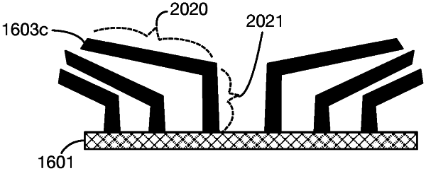
manufacturing the object by transmitting control signals to the anode array so that the material deposited onto the electrical connection pads forms columns that initiate on respective ones of the electrical connection pads at locations that are spaced apart along a surface of the semiconductor die by a first distance, and that are angled at a slant, relative to the surface of the semiconductor die and away from each other, so that connection points, defined by terminal ends of the columns, are spaced apart, in a direction parallel to the surface of the semiconductor die, by a second distance that is greater than the first distance.
|