| CPC H01L 21/30604 (2013.01) [B81C 1/00619 (2013.01); G02B 5/1857 (2013.01); H01L 21/308 (2013.01); H01L 21/3085 (2013.01); H01L 21/3086 (2013.01); H01L 31/028 (2013.01); B82Y 20/00 (2013.01); B82Y 40/00 (2013.01); C09K 13/08 (2013.01); G02B 5/1838 (2013.01); H01L 31/1804 (2013.01); Y02P 70/50 (2015.11)] | 9 Claims |
|
1. A method for fabricating photonic device elements by means of metal assisted chemical etching in gas phase, the method comprising the following steps:
(a) providing a semiconductor substrate and a patterned metal layer on the semiconductor substrate;
(b) exposing the semiconductor substrate and the patterned metal layer to reactants in gas phase, the reactants including an oxidant gas and an etchant gas;
the oxidant gas comprising air and the etchant gas comprising hydrofluoric acid;
supplying the reactants in a continuous or pulsed flow to the semiconductor substrate and the patterned metal layer on the semiconductor substrate;
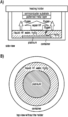
locally increasing a concentration of oxygen in the oxidant gas by decomposing H2O2 on a platinum surface, being a solid piece containing platinum immersed in a liquid solution containing H2O2, with a decomposition of H2O2 in the liquid phase on the platinum surface producing O2 in gas phase; and
wherein the liquid solution is placed in a container and the liquid is not in contact with the semiconductor substrate and the patterned metal on the semiconductor substrate.
|