| CPC H01F 27/2804 (2013.01) [H01F 17/0013 (2013.01); H01F 27/24 (2013.01); H01F 41/08 (2013.01)] | 22 Claims |
|
1. A method for constructing a solenoid inductor, comprising:
positioning an inner winding substantially around a magnetic core;
positioning an outer winding substantially around the inner winding;
using a layered process to perform said positioning the inner and outer windings;
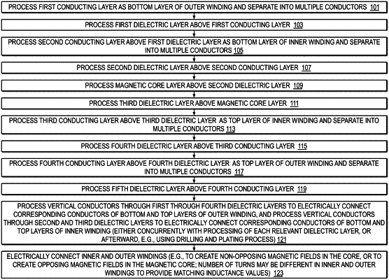
processing a first conducting layer that is a bottom layer of the outer winding;
processing a first dielectric layer above the first conducting layer;
processing a second conducting layer above the first dielectric layer that is a bottom layer of the inner winding;
processing a second dielectric layer above the second conducting layer;
processing a magnetic core layer above the second dielectric layer;
processing a third dielectric layer above the magnetic core layer;
processing a third conducting layer above the third dielectric layer that is a top layer of the inner winding;
processing a fourth dielectric layer above the third conducting layer;
processing a fourth conducting layer above the fourth dielectric layer that is a top layer of the outer winding; and
processing a fifth dielectric layer above the fourth conducting layer;
wherein the inner and outer windings are electrically connected.
|