| CPC G11C 5/06 (2013.01) [G11C 5/025 (2013.01); H01L 24/45 (2013.01)] | 20 Claims |
|
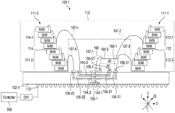
1. A solid state drive (SSD) comprising:
a substrate;
a first buffer chip disposed on the substrate;
a second buffer chip disposed on the first buffer chip;
a plurality of first nonvolatile memory chips;
a plurality of second nonvolatile memory chips; and
a controller configured to transmit a control signal to the plurality of first nonvolatile memory chips and the plurality of second nonvolatile memory chips through a first channel,
wherein the plurality of first nonvolatile memory chips are disposed between the first buffer chip and the plurality of second nonvolatile memory chips,
wherein the plurality of first nonvolatile memory chips are connected to the second buffer chip and are not connected to the first buffer chip, and
wherein the plurality of second nonvolatile memory chips are connected to the first buffer chip and are not connected to the second buffer chip.
|