| CPC G11C 17/18 (2013.01) [G11C 16/102 (2013.01); G11C 16/30 (2013.01); G11C 17/16 (2013.01)] | 18 Claims |
|
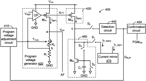
1. A program control circuit coupled to an antifuse control line of an antifuse-type one time programming memory cell array, the program control circuit generating a program voltage to program a selected memory cell of the antifuse-type one time programming memory cell array, the program control circuit comprising:
a program voltage generator, wherein an output terminal of the program voltage generator is coupled to the antifuse control line, wherein in a calibration phase of a program action, the program voltage generator generates a calibration voltage to the antifuse control line, wherein in at least one program phase of the program action, the program voltage generator generates the program voltage to the antifuse control line;
a program voltage adjustment circuit connected to the program voltage generator, wherein the program voltage adjustment circuit receives a rupture signal, and the program voltage adjustment circuit selectively adjusts the program voltage when the rupture signal is not activated;
a proportional current generator connected to the program voltage generator, wherein in the calibration phase, the proportional current generator generates a calibration current to a first node, wherein in the at least one program phase, the proportional current generator generates an operation current to the first node;
a current sampling circuit connected to the first node, wherein in the calibration phase, the current sampling circuit converts the calibration current into a sampling voltage, wherein in the at least one program phase, the current sampling circuit generates the calibration current according to the sampling voltage, and the calibration current flows from the first node to a ground terminal;
a first switch, wherein a first terminal of the first switch is connected to the first node;
a second switch, wherein a first terminal of the second switch is connected to the first node, wherein in the calibration phase, the first switch and the second switch are in an opened state, wherein in the at least one program phase, the first switch and the second switch are in a closed state;
a current mirror, wherein a current input terminal of the current mirror receives a first reference program current, a current mirrored terminal of the current mirror generates a second reference program current, and the current mirrored terminal is connected to a second terminal of the first switch, wherein in the at least one program phase, the second reference program current flows from the first node to the current mirrored terminal of the current mirror; and
a detection circuit connected to a second terminal of the second switch, wherein in the at least one program phase, the detection circuit judges a program current generated by the selected memory cell, wherein if the detection circuit judges that the program current is sufficient, the rupture signal is activated by the detection circuit.
|