| CPC G11C 16/16 (2013.01) [G11C 11/5635 (2013.01); G11C 11/5671 (2013.01); G11C 16/0483 (2013.01); H10B 41/27 (2023.02); H10B 43/27 (2023.02)] | 20 Claims |
|
1. A semiconductor memory device, comprising:
a source layer in a substrate and including a conductive material doped with first conductivity type impurities;
a channel structure on the substrate, the channel structure including a vertical insulation layer and a vertical channel layer, the channel structure extending in a first direction that is perpendicular to an upper surface of the substrate;
a plurality of gate electrodes on the source layer and spaced apart from each other in the first direction on a sidewall of the channel structure, wherein the plurality of gate electrodes includes
a first word line group including a first gate electrode and a second gate electrode that are continuously arranged in the first direction, and
a second word line group including a third gate electrode and a fourth gate electrode that are continuously arranged in the first direction; and
a common source line electrically connected to the source layer,
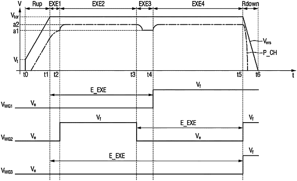
wherein the semiconductor memory device is configured to, in response to a voltage of the common source line reaching a target voltage,
cause an inhibition voltage to be applied to the second word line group and an erase voltage to be applied to the first word line group in a first interval during an erase operation, and
cause the inhibition voltage to be applied to the first word line group and the erase voltage to be applied to the second word line group in a second interval after the first interval during the erase operation.
|