| CPC G09G 3/3275 (2013.01) [G09G 3/3266 (2013.01); H10K 59/353 (2023.02)] | 21 Claims |
|
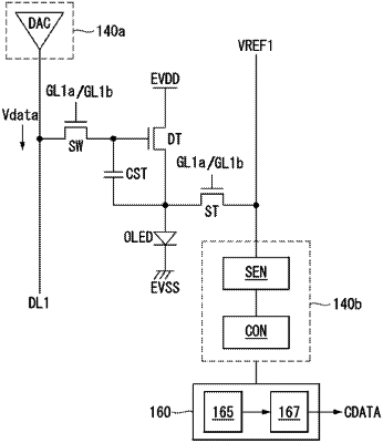
1. A light emitting display device, comprising:
a display panel including M subpixels sharing a sensing line, wherein M is an integer equal to or greater than 2; and
a circuit configured to sense one or more elements included in at least one of the M subpixels through the sensing line,
wherein the M sub-pixels are initialized based on an initialization voltage during an initial period,
wherein the M sub-pixels are sensed based on a sensing voltage during a data writing period,
wherein each of the M subpixels includes a switching transistor and a sensing transistor commonly connected to one scan line,
wherein in one of the M pixels, the switching transistor and the sensing transistor are simultaneously turned on in response to a scan signal, and
wherein in the one of the M pixels, an amount of turn-on time of the switching transistor and the sensing transistor during the initial period is longer than an amount of turn-on time of the switching transistor and the sensing transistor during the data writing period.
|