| CPC G09G 3/035 (2020.08) [G09G 2300/0426 (2013.01); G09G 2330/028 (2013.01)] | 23 Claims |
|
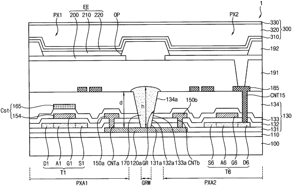
1. A display device, comprising:
a first pixel area on which a first pixel is disposed;
a second pixel area on which a second pixel is disposed, the second pixel area being disposed adjacent to the first pixel area along a first direction;
a lower connection line connecting the first pixel and the second pixel, and crossing the first pixel area and the second pixel area;
an inorganic insulating layer disposed on the lower connection line and having a groove disposed between the first pixel area and the second pixel area, and exposing an upper surface of the lower connection line; and
an organic insulating layer filling the groove of the inorganic insulating layer.
|
|
16. A display device, comprising:
a substrate, the substrate including a first pixel area and a second pixel area disposed adjacent to the first pixel area along a first direction;
a first lower connection line disposed on the substrate and crossing the first pixel area and the second pixel area;
a first inorganic insulating layer disposed on the first lower connection line and having a first opening disposed between the first pixel area and the second pixel area;
a first conductive line disposed on the first inorganic insulating layer in the first pixel area and being connected to the first lower connection line through a first contact hole formed through the first inorganic insulating layer;
a second conductive line disposed on the first inorganic insulating layer in the second pixel area and being connected to the first lower connection line through a second contact hole formed through the first inorganic insulating layer;
a second inorganic insulating layer disposed on the first conductive line and the second conductive line, and having a second opening overlapping the first opening in a plan view; and
an organic insulating layer filling the first opening of the first inorganic insulating layer and the second opening of the second inorganic insulating layer.
|
|
19. A display device, comprising:
a plurality of pixel areas;
a lower connection line crossing the plurality of pixel areas;
an inorganic insulating layer disposed on the lower connection line and having a groove disposed between adjacent pixel areas of the plurality of pixel areas and exposing an upper surface of the lower connection line; and
an organic insulating layer filling the groove of the inorganic insulating layer.
|
|
23. A display device, comprising:
a substrate, the substrate including a first pixel area on which a first pixel is disposed and a second pixel area on which a second pixel is disposed, emission areas of the first pixel and the second pixel each being defined by an opening of a pixel defining layer in which an emission layer is disposed between a pixel electrode and an opposite electrode;
a lower connection line disposed on the substrate and crossing the first pixel area and the second pixel area;
an inorganic insulating layer disposed on the lower connection line and having a groove disposed between the first pixel area and the second pixel area and exposing an upper surface of the lower connection line; and
an organic insulating layer disposed between the lower connection line and the pixel defining layer, and filling the groove of the inorganic insulating layer.
|