US 11,880,582 B2
Memory device having improved program and erase operations and operating method of the memory device
Byung In Lee, Hwaseong-si (KR); Hee Joung Park, Seoul (KR); Keon Soo Shim, Icheon-si (KR); Sang Heon Lee, Chungcheongbuk-do (KR); and Jae Il Tak, Seoul (KR)
Assigned to SK hynix Inc., Icheon-si (KR)
Filed by SK hynix Inc., Icheon-si (KR)
Filed on Feb. 11, 2021, as Appl. No. 17/173,794.
Application 17/173,794 is a continuation in part of application No. 16/510,071, filed on Jul. 12, 2019, granted, now 10,950,306.
Claims priority of application No. 10-2019-0000453 (KR), filed on Jan. 2, 2019.
Prior Publication US 2021/0165603 A1, Jun. 3, 2021
Int. Cl. G11C 11/34 (2006.01); G06F 3/06 (2006.01)
CPC G06F 3/0655 (2013.01) [G06F 3/0604 (2013.01); G06F 3/0652 (2013.01); G06F 3/0679 (2013.01)] 10 Claims
OG exemplary drawing
 
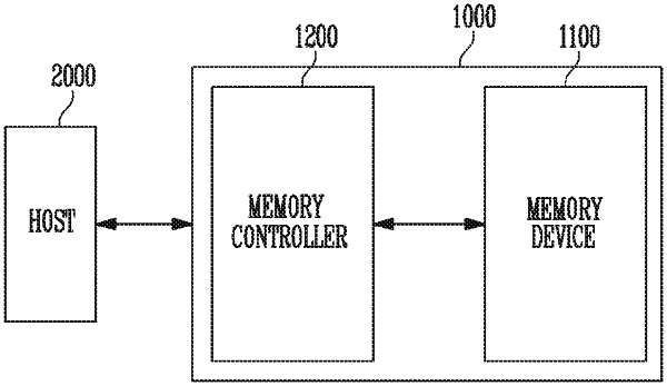
1. A method for operating a memory device, the method comprising:
providing a memory block including at least one source select transistor coupled between a source line and a bit line, a plurality of memory cells, and a drain select transistor;
controlling a source select line coupled to the at least one source select transistor and a plurality of word lines coupled to the plurality of memory cells to be in a floating state; and
after controlling the at least one source select transistor to be in the floating state, applying an erase voltage to the source line and the bit line.