| CPC G06F 3/0412 (2013.01) [H10K 50/805 (2023.02); H10K 59/40 (2023.02); G06F 3/0443 (2019.05); G06F 3/0446 (2019.05); H10K 50/8426 (2023.02)] | 15 Claims |
|
1. A display device comprising:
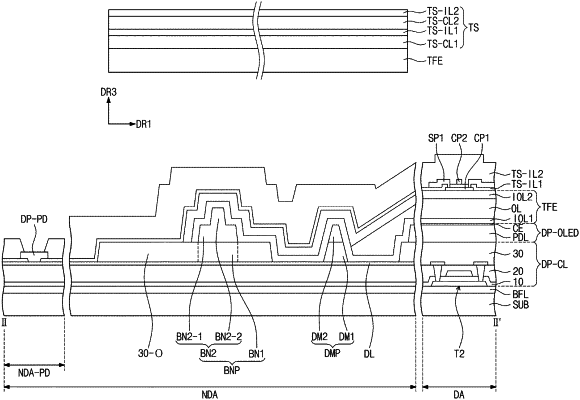
a base layer comprising a display area and a non-display area disposed outside the display area;
an intermediate inorganic layer disposed on the base layer and overlapping the display area and the non-display area;
an intermediate organic layer disposed on the intermediate inorganic layer to expose a portion of the intermediate inorganic layer within the non-display area in a plan view;
a light emitting diode disposed on the intermediate organic layer and overlapping the display area;
a thin film encapsulation layer disposed on the light emitting diode and comprising a first encapsulation inorganic layer, an encapsulation organic layer on the first encapsulation inorganic layer, and a second encapsulation inorganic layer on the encapsulation organic layer, at least one of the first encapsulation inorganic layer and the second encapsulation inorganic layer comprising a first region overlapping the display area and a second region overlapping the non-display area and having a thickness less than that of the first region;
an electrode disposed on the thin film encapsulation layer;
a first inorganic layer on the thin film encapsulation layer and overlapping the display area and the non-display area, the first inorganic layer contacting the portion of the intermediate inorganic layer exposed by the intermediate organic layer; and
a second inorganic layer is disposed between the second encapsulation inorganic layer and the first inorganic layer.
|