| CPC G05F 1/575 (2013.01) [G05F 1/56 (2013.01)] | 20 Claims |

|
1. A voltage regulator circuit comprising:
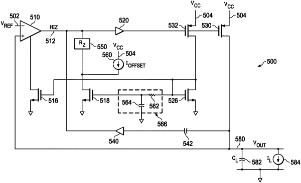
a first amplifier having first and second amplifier inputs, a bias terminal and a first amplifier output, wherein the first amplifier input is coupled to a voltage reference, and the second amplifier input is coupled to an output voltage terminal;
a first transistor having first and second transistor current terminals and a first control terminal, wherein the first transistor current terminal is coupled to a supply voltage terminal, and the first control terminal is coupled to the first amplifier output;
a second transistor having third and fourth transistor current terminals and a second control terminal, wherein the third transistor current terminal is coupled to the supply voltage terminal, the second control terminal is coupled to the first control terminal, and the fourth transistor current terminal is coupled to the output voltage terminal;
a third transistor having fifth and sixth transistor current terminals and a third control terminal, wherein the fifth transistor current terminal and the third control terminal are coupled to the second transistor current terminal, and the sixth transistor current terminal is coupled to a ground terminal;
a fourth transistor having seventh and eighth transistor current terminals and a fourth control terminal, wherein the fourth control terminal is coupled to the third control terminal, and the eighth transistor current terminal is coupled to the ground terminal;
a fifth transistor having ninth and tenth transistor current terminals and a fifth control terminal, wherein the ninth transistor current terminal is coupled to the bias terminal of the first amplifier, the fifth control terminal is coupled to the third control terminal, and the tenth transistor current terminal is coupled to the ground terminal;
a dynamic R-C network coupled between the first amplifier output and the seventh transistor current terminal; and
a buffer having a buffer input and a buffer output, wherein the buffer input is coupled to the output voltage terminal.
|