US 11,880,123 B2
Structured light projector and electronic device including the same
Hyeonsoo Park, Suwon-si (KR); Seunghoon Han, Seoul (KR); and Minkyung Lee, Suwon-si (KR)
Assigned to SAMSUNG ELECTRONICS CO., LTD., Suwon-si (KR)
Filed by SAMSUNG ELECTRONICS CO., LTD., Suwon-si (KR)
Filed on Nov. 18, 2022, as Appl. No. 17/990,543.
Application 17/990,543 is a continuation of application No. 17/352,998, filed on Jun. 21, 2021, granted, now 11,592,733.
Application 17/352,998 is a continuation of application No. 16/441,559, filed on Jun. 14, 2019, granted, now 11,067,877, issued on Jul. 20, 2021.
Claims priority of provisional application 62/758,064, filed on Nov. 9, 2018.
Claims priority of application No. 10-2019-0017960 (KR), filed on Feb. 15, 2019.
Prior Publication US 2023/0080866 A1, Mar. 16, 2023
This patent is subject to a terminal disclaimer.
Int. Cl. G03B 21/20 (2006.01); H04N 9/31 (2006.01)
CPC G03B 21/2013 (2013.01) [H04N 9/3152 (2013.01)] 13 Claims
OG exemplary drawing
 
1. A structured light projector comprising:
a light source configured to emit light, the light source comprising a plurality of light-emitting elements; and
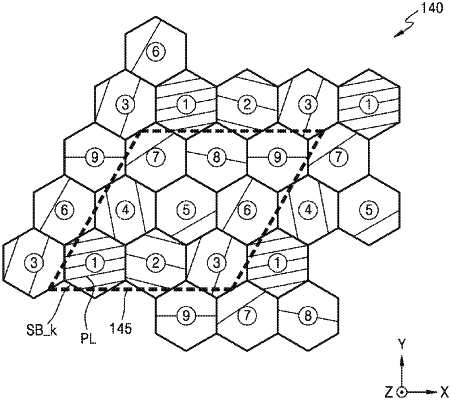
a nanostructure array configured to form a dot pattern based on the light emitted by the plurality of light-emitting elements, the nanostructure array comprising a plurality of super cells,
wherein each of the plurality of super cells comprises a plurality of sub cells which are sub-divided areas of each of the plurality of super cells, wherein each of the plurality of sub cells comprises a plurality of nanostructures, and
wherein a distance between the light source and the nanostructure array is determined by a lattice constant of the plurality of super cells and a central wavelength of the light emitted by the light source.