| CPC G02F 1/13725 (2013.01) [B32B 7/023 (2019.01); B32B 7/12 (2013.01); B32B 27/08 (2013.01); B32B 27/306 (2013.01); B32B 27/365 (2013.01); B60J 1/001 (2013.01); B60J 3/04 (2013.01); G02F 1/1337 (2013.01); G02F 1/133531 (2021.01); G02F 1/134309 (2013.01); B32B 2255/10 (2013.01); B32B 2255/20 (2013.01); B32B 2305/55 (2013.01); B32B 2307/42 (2013.01); B32B 2551/00 (2013.01); B60J 7/043 (2013.01); G02F 2202/04 (2013.01); G02F 2203/01 (2013.01)] | 14 Claims |
|
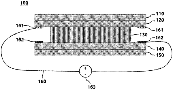
1. An optical element, comprising:
an optical film having a first base film, a first electrode layer,
a light modulation layer, a second electrode layer, and a second base film arranged in sequential order, and an insulating layer; and
a transmittance control device,
wherein the first and second electrode layers each comprise a first region and a second region, wherein the first region is configured to apply an electric field to the light modulation layer and the second region is configured to connect the electrode layer to an external power source that supplies power to the first region, wherein the external power source is connected to the second region via the transmittance control device, wherein the second region is at the edge of each of the first and second electrode layers, wherein a terminal is present in the second region to connect the electrode layer to the external power source, wherein the light modulation layer does not overlie the second region,
wherein the insulating layer is positioned on the second regions of the first and second base films, and between the first and second electrode layers,
wherein the second region on the first base film comprises A and B regions formed on opposite edges of the first base film, respectively, and the second region on the second base film comprises C and D regions formed on opposite edges of the second base film, respectively,
the A region and the C region face each other, and the B region and the D region face each other,
wherein the optical element is configured to switch between a gradation mode when the A and C regions or the B and D regions are connected to an external power source to generate an electric field in the first region and a uniform transparent mode when the A and D regions or the B and C regions are connected to an external power source to generate an electric field in the first region,
wherein the external power source is directly connected to only one of the A and B regions, and is directly connected to only one of the C and D regions, and
wherein the transmittance control device comprises a driving device configured to select a site on the second regions to which the external power source is connected.
|