| CPC G01R 31/318536 (2013.01) [G01R 31/31855 (2013.01); G01R 31/31858 (2013.01); G01R 31/318525 (2013.01); G01R 31/318563 (2013.01); G01R 31/318566 (2013.01)] | 25 Claims |
|
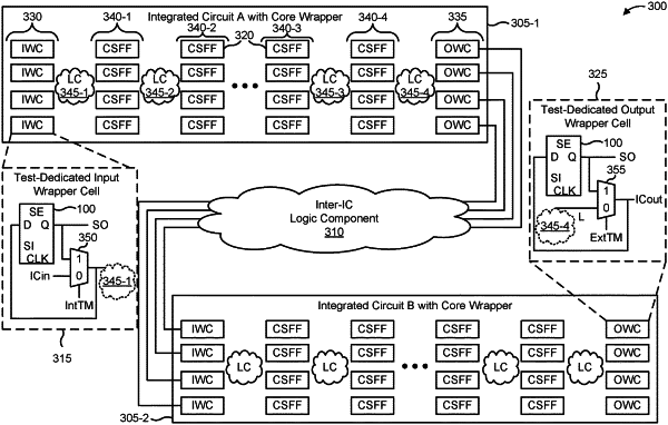
1. An integrated circuit, comprising:
a plurality of input scan flip-flops arranged in a plurality of input scan flip-flop stages that includes at least a first input scan flip-flop stage and a second input scan flip-flop stage,
wherein inputs to a first plurality of input scan flip-flops included in the first input scan flip-flop stage are connected to inputs of the integrated circuit, and
wherein inputs to a second plurality of input scan flip-flops included in the second input scan flip-flop stage are connected to outputs of a logic component that is connected to outputs of the first plurality of input scan flip-flops; and
a plurality of output scan flip-flops arranged in a plurality of output scan flip-flop stages that includes at least a first output scan flip-flop stage and a second output scan flip-flop stage,
wherein outputs from a first plurality of output scan flip-flops included in the first output scan flip-flop stage are connected to outputs of the integrated circuit, and
wherein outputs from a second plurality of output scan flip-flops included in the second output scan flip-flop stage are connected to inputs of a logic component that is connected to inputs of the first plurality of output scan flip-flops.
|