| CPC G01R 31/312 (2013.01) | 17 Claims |
|
1. An apparatus, comprising:
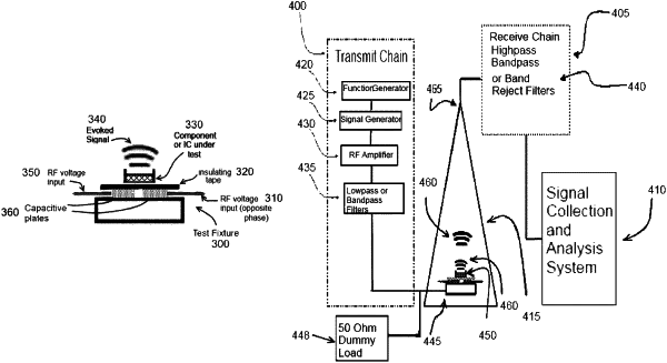
a testing fixture configured to receive an electronic part specimen under test (PSUT) and energize the PSUT without a direct pin-to-metal electrical contact with the PSUT;
a shielded enclosure having an interior and exterior, the testing fixture positioned within the interior; a receiving antenna positioned within the interior;
a transmission chain connected to the testing fixture, the transmission chain at least including a filter to pass a high power signal to the testing fixture;
a receiving chain connected to the receiving antenna, the receiving chain at least including a filter to pass a low power signal;
and an analysis unit connected to the receiving chain to analyze the low power signal,
wherein the testing fixture comprises a capacitive member to capacitively energize the PSUT.
|