| CPC H10K 71/80 (2023.02) [B32B 7/12 (2013.01); B32B 27/08 (2013.01); B32B 27/281 (2013.01); B32B 27/36 (2013.01); B32B 37/02 (2013.01); B32B 37/12 (2013.01); B32B 38/0004 (2013.01); B32B 43/006 (2013.01); H10K 59/12 (2023.02); H10K 59/88 (2023.02); H10K 71/00 (2023.02); H10K 77/111 (2023.02); B32B 2367/00 (2013.01); B32B 2379/08 (2013.01); B32B 2457/20 (2013.01); H10K 59/1201 (2023.02); H10K 71/851 (2023.02); H10K 2102/311 (2023.02)] | 8 Claims |
|
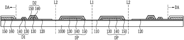
1. A manufacturing method of a display device, comprising:
preparing a substrate including a plurality of display modules and a plurality of dummy patterns disposed between the plurality of display modules; and
cutting the substrate along a cutting line and separating the substrate into individual display modules,
wherein the plurality of dummy patterns are disposed along a direction parallel to the cutting line, and each of the plurality of dummy patterns is provided with a groove disposed along a direction perpendicular to the cutting line.
|