| CPC H10K 71/00 (2023.02) [H10K 59/131 (2023.02); H10K 59/1201 (2023.02)] | 17 Claims |
|
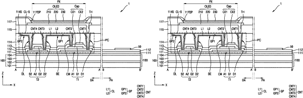
1. A method of manufacturing a display device, the method comprising:
preparing a substrate having a first area and a second area surrounding at least a portion of the first area;
forming a semiconductor layer in the first area on the substrate;
forming a first insulating layer covering the semiconductor layer;
forming a gate electrode layer that at least partially overlaps the semiconductor layer;
forming a pad electrode layer in the second area on the substrate;
forming a second insulating layer covering the gate electrode layer;
forming contact holes that at least partially expose the semiconductor layer and the gate electrode layer; and
forming a conductive layer positioned in the contact holes and comprising a first layer and a second layer, wherein the first layer and the second layer of the conductive layer comprise different materials from each other,
wherein the forming of the conductive layer comprises:
forming a first layer material covering the second insulating layer, the contact holes, and the pad electrode layer;
forming a second layer material covering the first layer material;
removing a portion of the first layer material and a portion of the second layer material to expose the second insulating layer; and
completely removing the first layer material and the second layer material positioned in the second area.
|