| CPC H10K 59/90 (2023.02) [G01K 3/14 (2013.01); G09G 3/3225 (2013.01); H10N 19/00 (2023.02); G09G 2320/041 (2013.01); G09G 2340/04 (2013.01)] | 19 Claims |
|
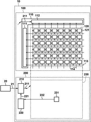
1. A light emitting device in which are stacked a first substrate, including a light emitting area where a plurality of light emitting elements are arranged, and a second substrate, where a first temperature detector configured to detect a temperature of the first substrate is arranged,
wherein in an orthogonal projection with respect to a main surface of the first substrate where the light emitting area is arranged, a plurality of temperature detectors including the first temperature detector are arranged in an overlapping area of the second substrate overlapping the light emitting area.
|