| CPC H10K 59/126 (2023.02) [H01L 27/124 (2013.01); H01L 27/1255 (2013.01); H01L 27/1225 (2013.01)] | 15 Claims |
|
1. A display panel, comprising:
a substrate;
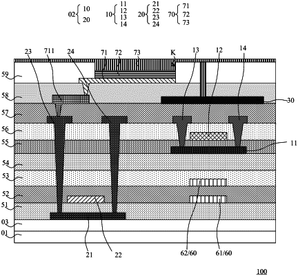
a driving circuit including an oxide transistor and a silicon transistor disposed on the substrate, wherein the oxide transistor includes a first active layer; and
a first light blocking layer, wherein an orthographic projection of the first light blocking layer on the substrate at least overlaps an orthographic projection of the first active layer on the substrate; power signal lines, wherein: at least a portion of the power signal lines is disposed in a layer same as the first light blocking layer; the oxide transistor includes a first gate at a side of the first active layer away from the substrate; and the first light blocking layer is multiplexed as the first gate; wherein the power signal lines include: first sub power signal lines extending in a first direction and arranged in a second direction, and second sub power signal lines extending in the second direction and arranged in the first direction; the first sub power signal lines and the second sub power signal lines transmit same signals; the display panel further includes data signal lines; the data signal lines extend in the second direction and are arranged in the first direction; and the first sub power signal lines and the first light blocking layer are disposed in a same layer; wherein the second sub power signal lines include a first portion and a second portion; and in the first direction, the first portion at least does not overlap the second portion; a capacitor, wherein the second gate is disposed in a layer same as any electrode plate of the capacitor.
|