| CPC H05K 1/0245 (2013.01) [H01R 12/7082 (2013.01); H01R 12/716 (2013.01); H05K 1/0219 (2013.01); H05K 1/0251 (2013.01); H05K 1/115 (2013.01); H05K 3/429 (2013.01); H05K 1/0225 (2013.01); H05K 2201/096 (2013.01); H05K 2201/09727 (2013.01); H05K 2201/09845 (2013.01)] | 5 Claims |
|
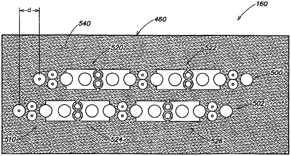
1. A printed circuit board comprising:
a plurality of layers including conductive layers separated by dielectric layers; and
a connector footprint formed on the plurality of layers, the connector footprint comprising:
a plurality of columns of pairs of signal vias, the pairs of signal vias in adjacent columns of the plurality of columns being offset in a direction of the columns; and
at least one shadow via disposed in the columns between adjacent pairs of signal vias, wherein the at least one shadow via is plated or filled with a conductive material.
|