| CPC H04N 23/52 (2023.01) [G01S 17/894 (2020.01); H04N 23/51 (2023.01); H04N 23/55 (2023.01); H04N 23/56 (2023.01); H01L 27/14618 (2013.01)] | 18 Claims |

|
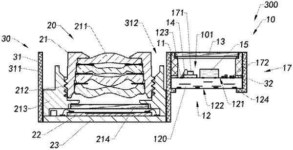
1. A projection module, comprising:
a transmitting circuit board;
a frame-shaped support, wherein the support is disposed on the transmitting circuit board and has an opening at its top surface;
an optical element, wherein the optical element is attached to the opening of the support, and an accommodating space is formed above the transmitting circuit board by means of the optical element and the support;
at least one projection unit, wherein the projection unit is disposed in the accommodating space, and the projection unit is conductively attached to the transmitting circuit board; and
at least one driver chip, wherein the driver chip is packaged into the accommodating space, the driver chip is conductively connected to the transmitting circuit board, the driver chip is on the same side as the projection unit, and the driving chip sends a light control signal to the projection unit based on the transmitting circuit board;
wherein the transmitting circuit board has an upper end surface and a lower end surface, wherein the driver chip is attached to the upper end surface of the transmitting circuit board in a manner adjacent to the projection unit; and
the transmitting circuit board comprises:
a transmitting circuit substrate;
a plurality of upper solder joints, wherein the upper solder joints are disposed on an upper end of the transmitting circuit substrate;
a plurality of lower solder joints, wherein the lower solder joints are disposed on a lower end of the transmitting circuit substrate; and
a plurality of conduction circuits, wherein the conduction circuits electrically connect the upper solder joints and the lower solder joints, and wherein the driver chip is conductively connected to the conduction circuits through the upper solder joints, and the lower solder joints are electrically connected to the upper solder joints through the conduction circuits.
|