| CPC H04L 25/4917 (2013.01) [H03K 3/037 (2013.01); H03K 5/02 (2013.01); H04B 1/16 (2013.01); H04L 27/06 (2013.01)] | 20 Claims |
|
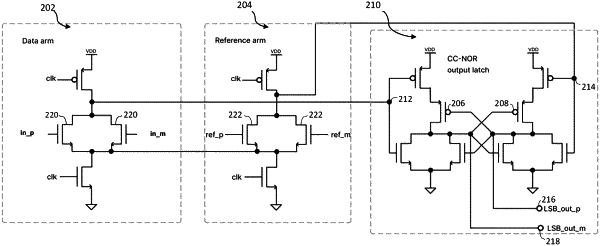
1. A sampling circuit comprising:
a data sense amplifier circuit;
a reference sense amplifier circuit directly connected with the data sense amplifier circuit; and
a latch circuit configured to receive a first input from the data sense amplifier circuit and a second input from the reference sense amplifier circuit, the latch circuit further configured to generate a least significant bit output based upon, at least in part, the first input and the second input.
|