| CPC H03K 19/1737 (2013.01) [H03K 17/693 (2013.01); H03K 19/00361 (2013.01); H03K 19/1776 (2013.01)] | 20 Claims |
|
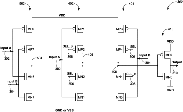
1. An electronic device, comprising:
a first multiplexer branch configured to generate a first output signal from a first selection signal, a first inverse signal, and a first input signal, wherein the first inverse signal is substantially complementary to the first selection signal;
a second multiplexer branch configured to generate a second output signal from the first selection signal, the first inverse signal, and a second input signal;
a modulation circuit configured to generate a logic output signal from the first input signal and the second input signal, independently of the first selection signal and the first inverse signal; and
an output interface coupled to the modulation circuit, the first multiplexer branch, and the second multiplexer branch, wherein the output interface is configured to generate a multiplexed output signal tracking one of the first input signal and the second input signal based on the first output signal, the second output signal, and the logic output signal.
|