| CPC H01L 33/62 (2013.01) [H01L 24/05 (2013.01); H01L 24/13 (2013.01); H01L 24/81 (2013.01); H01L 2224/0401 (2013.01); H01L 2224/0508 (2013.01); H01L 2224/05082 (2013.01); H01L 2224/05083 (2013.01); H01L 2224/05084 (2013.01); H01L 2224/05124 (2013.01); H01L 2224/05144 (2013.01); H01L 2224/05147 (2013.01); H01L 2224/05155 (2013.01); H01L 2224/05171 (2013.01); H01L 2224/05184 (2013.01); H01L 2224/0519 (2013.01); H01L 2224/13026 (2013.01); H01L 2224/1308 (2013.01); H01L 2224/13082 (2013.01); H01L 2224/13083 (2013.01); H01L 2224/13084 (2013.01); H01L 2224/1319 (2013.01); H01L 2224/13193 (2013.01); H01L 2224/13209 (2013.01); H01L 2224/13211 (2013.01); H01L 2224/13213 (2013.01); H01L 2224/13239 (2013.01); H01L 2224/13244 (2013.01); H01L 2224/13247 (2013.01); H01L 2224/13255 (2013.01); H01L 2224/13561 (2013.01); H01L 2224/13562 (2013.01); H01L 2224/1357 (2013.01); H01L 2224/1369 (2013.01); H01L 2224/81011 (2013.01); H01L 2224/8102 (2013.01); H01L 2224/81193 (2013.01); H01L 2224/81203 (2013.01); H01L 2224/81224 (2013.01); H01L 2224/81355 (2013.01); H01L 2224/8181 (2013.01); H01L 2924/01029 (2013.01); H01L 2924/01047 (2013.01); H01L 2924/01049 (2013.01); H01L 2924/0105 (2013.01); H01L 2924/01079 (2013.01); H01L 2924/01083 (2013.01); H01L 2924/014 (2013.01); H01L 2924/12041 (2013.01); H01L 2933/0066 (2013.01)] | 20 Claims |
|
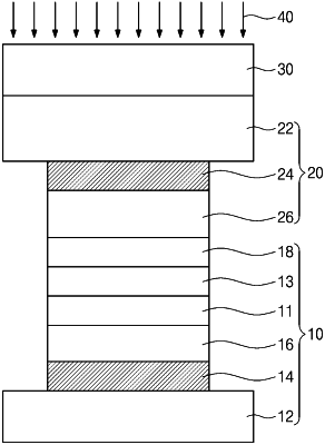
1. A method of fabricating a semiconductor package, the method comprising:
preparing a lower element including a lower substrate, a lower electrode on the lower substrate, an under bump metallurgy (UBM) layer on the lower electrode, and a reducing agent layer on the UBM layer;
providing an upper element including an upper substrate, an upper electrode on the upper substrate, and a solder bump layer on the upper electrode;
providing a pressing member on the upper substrate to press the upper substrate to the lower substrate; and
providing a laser beam passing through the pressing member to the upper substrate to form the UBM layer, the reducing agent layer, and the solder bump layer as an intermetallic compound layer by using a conductive heat of the upper substrate and the upper electrode.
|