| CPC H01L 33/007 (2013.01) [H01L 25/0753 (2013.01); H01L 33/0095 (2013.01); H01L 2933/0016 (2013.01)] | 10 Claims |
|
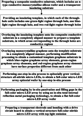
1. A method for monolithic integration preparation of a full-color nitride semiconductor micro light-emitting diode (micro-LED) array, comprising the steps of
1) preparing a composite conductive substrate, comprising:
1-a) providing a transparent insulating substrate, wherein a material for the transparent insulating substrate has a bandgap greater than 5.0 eV and does not absorb ultraviolet light with a wavelength greater than 250 nm; and
1-b) providing an n-type conductive monocrystalline silicon wafer with a resistivity less than 0.01 ohm·cm; performing polishing on one side of the n-type conductive monocrystalline silicon wafer to form a polished surface, thinning a non-polished surface of the n-type conductive monocrystalline silicon wafer, and attaching the n-type conductive monocrystalline silicon wafer onto the transparent insulating substrate, with the polished surface facing upwards, to form the composite conductive substrate, wherein an outer periphery of the n-type conductive monocrystalline silicon wafer has a same shape as an outer periphery of the transparent insulating substrate;
2) providing an insulating template,
wherein the insulating template is a flat panel made of an electrically insulating material; an outer periphery of the insulating template has a same shape as an outer periphery of the composite conductive substrate; the insulating template is divided into a plurality of through hole units that are arranged closely in a two-dimensional manner; an outer periphery of each of the through hole units is in a plane shape of square; each of the through hole units comprises four circular through holes inside with a depth equal to a thickness of the insulating template, namely, one green-light region through hole, one blue-light region through hole, and two red-light region through holes; the green-light region through hole and the blue-light region through hole are respectively located at a pair of diagonal corners of the square, and the two red-light region through holes are respectively located at the other pair of diagonal corners of the square;
3) preparing a template substrate, comprising:
3-a) overlaying the insulating template onto the composite conductive substrate in a completely aligned manner;
3-b) preparing a protective layer on the insulating template, such that the protective layer is formed on the n-type conductive monocrystalline silicon wafer in areas corresponding to the circular through holes of the insulating template, while no protective layer is formed in areas not corresponding to the circular through holes of the insulating template;
3-c) removing the insulating template, and performing ion implantation on the n-type conductive monocrystalline silicon wafer, such that ions are implanted into the areas of the n-type conductive monocrystalline silicon wafer which are not covered by the protective layer, thereby increasing resistivity and making the areas electrically insulating;
3-d) performing chemical cleaning on the composite conductive substrate after ion implantation to remove the protective layer, wherein the areas corresponding to the circular through holes of the insulating template remain conductive, while remaining areas become electrically insulating, thus completing modification of the n-type conductive monocrystalline silicon wafer to obtain the template substrate; and
3-e) corresponding to the insulating template, providing a plurality of pixel regions arranged closely in a two-dimensional manner on the n-type conductive monocrystalline silicon wafer of the template substrate, wherein each of the pixel regions comprises four circular conductive regions, namely, two red-light conductive regions, one green-light conductive region, and one blue-light conductive region, and the rest being an insulating region;
4) preparing a customized template graphene substrate, comprising
4-a) providing monocrystalline graphene, wherein an outer periphery of the monocrystalline graphene has a same shape as the template substrate, and the monocrystalline graphene has a thickness of 3 to 6 atomic layers;
4-b) overlaying the monocrystalline graphene onto the template substrate in a completely aligned manner;
4-c) overlaying the insulating template onto the monocrystalline graphene in a completely aligned manner, wherein the one green-light region through hole, the one blue-light region through hole, and the two red-light region through holes in each of the through hole units of the insulating template are respectively precisely aligned with the one green-light conductive region, the one blue-light conductive region, and the two red-light conductive regions in each of the pixel regions of the n-type conductive monocrystalline silicon wafer;
4-d) thinning the monocrystalline graphene in areas corresponding to blue-light region through holes and green-light region through holes, until the areas have a thickness of one atomic layer;
4-e) performing uniform nitrogen atom doping on the monocrystalline graphene in areas corresponding to the blue-light region through holes, the green-light region through holes, and red-light region through holes, wherein the monocrystalline graphene after the uniform nitrogen atom doping exhibits ultraviolet absorption within a range of 240 nm to 270 nm;
4-f) depositing an AlON layer on the monocrystalline graphene in areas corresponding to the blue-light region through holes, such that a nitride epitaxial layer grown thereon has a metal lattice polarity; and
4-g) cutting edges of the monocrystalline graphene that correspond to the blue-light region through holes, the green-light region through holes, and the red-light region through holes of the insulating template, wherein the cutting is performed only on the monocrystalline graphene; and removing the insulating template to obtain the customized template graphene substrate,
wherein blue-region graphene array elements, green-region graphene array elements, and red-region graphene array elements are formed on the monocrystalline graphene in areas respectively corresponding to the blue-light region through holes, the green-light region through holes, and the red-light region through holes, and an insulating-region graphene array element is formed among the blue-region graphene array elements, the green-region graphene array elements, and the red-region graphene array elements, thereby forming graphene array units each comprising one blue-region graphene array element, one green-region graphene array element, two red-region graphene array elements, and an insulating-region graphene array element; and
wherein the one blue-region graphene array element, the one green-region graphene array element, and the two red-region graphene array elements in each of the graphene array units on the n-type conductive monocrystalline silicon wafer of the customized template graphene substrate have surface properties different from each other;
5) preparing a full-color micro-LED array epitaxial wafer, comprising
placing the customized template graphene substrate into a metal organic chemical vapor deposition system, epitaxially growing a vertical-structure all-nitride material on the customized template graphene substrate through one-step in-situ process, thereby obtaining the full-color micro-LED array epitaxial wafer through the one-step in-situ process,
wherein a multiple quantum well (MQW) of the vertical-structure all-nitride material comprises multiple periods of InGaN potential wells and GaN potential barriers;
due to the different surface properties of the blue-region graphene array elements, the green-region graphene array elements, and the red-region graphene array elements on the customized template graphene substrate, vertical-structure all-nitride materials grown thereon have different lattice polarities, stress states, and In compositions in MQW structures, and thereby different central emission wavelengths, and therefore a vertical-structure monocrystalline metal-polar blue-light-emitting nitride, a vertical-structure monocrystalline nitrogen-polar green-light-emitting nitride, and a vertical-structure monocrystalline stress-relaxed nitrogen-polar red-light-emitting nitride are grown respectively on the blue-region graphene array elements, the green-region graphene array elements, and the red-region graphene array elements, to form a blue-light-emitting micro-LED, a green-light-emitting micro-LED, and a red-light-emitting micro-LED, as well as an area without micro-LEDs, which constitute a micro-LED pixel unit; and
the blue-light-emitting micro-LED, the green-light-emitting micro-LED, and the red-light-emitting micro-LED are micrometer-sized pillars;
6) packaging, comprising
providing sidewall protection for the full-color micro-LED array epitaxial wafer by using an in-situ passivation packaging technology, and filling gaps in the full-color micro-LED array by using an in-situ total internal reflection metal packaging technology, to obtain a flat full-color micro-LED array wafer; and
7) preparing a transparent electrode, comprising
preparing the transparent electrode on a surface of the flat full-color micro-LED array wafer by using a mask deposition method, and bonding the flat full-color micro-LED array wafer onto a drive circuit board by using a bottom electrode bonding technology, to achieve a vertical-structure full-color nitride micro-LED array with top light emission.
|