| CPC H01L 31/035236 (2013.01) [H01L 31/03046 (2013.01); H01L 31/109 (2013.01); H01L 31/1844 (2013.01)] | 20 Claims |
|
1. An infrared detector, comprising:
an absorber region formed from a first semiconductor material with a first lattice constant, wherein the first semiconductor material produces charge carriers in response to infrared light, and wherein the first semiconductor material is a ternary alloy of the form AB1-xCx, where A is a first material, B is a second material, and C is a third material;
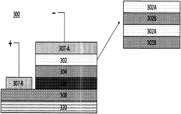
a barrier region disposed on the absorber region, wherein the barrier region is a superlattice comprising: (i) a plurality of first barrier region layers comprising the first semiconductor material, and (ii) a plurality of second barrier region layers comprising a second semiconductor material that is different from the first semiconductor material, wherein the plurality of first barrier region layers are alternatingly arranged with the plurality of second barrier region layers; and
a contact region disposed on the barrier region, wherein the contact region is another superlattice comprising: (i) a plurality of first contact region layers comprising the first semiconductor material, and (ii) a plurality of second contact region layers comprising the second semiconductor material, wherein the plurality of first contact region layers are alternatingly arranged with the plurality of second contact region layers,
wherein the second semiconductor material is lattice matched to the first semiconductor material resulting in the absorber region, the barrier region, and the contact region being unstrained.
|