| CPC H01L 29/8613 (2013.01) [H01L 29/66121 (2013.01); H01L 29/66136 (2013.01)] | 22 Claims |
|
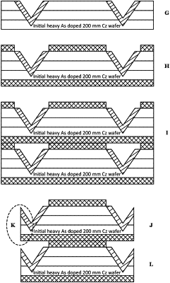
1. A method of making a stacked semiconductor diode comprising:
a) preparing initial heavy doped silicon <100> wafers for the growth of lower doped layers thereupon;
b) sequentially epitaxially growing alternating blanket n-doped and p-doped layers on the initial heavy doped silicon <100> wafers thus yielding wafer-sized diode structures;
c) forming a plurality of side terminating mesas on each wafer-sized diode structure defining individual diodes, wherein each respective side terminating mesa slopes to terminate diode sides;
d) depositing electrically conducting layers on both sides of each respective wafer-sized diode structure having the plurality of side terminating mesas formed therein;
e) stacking a predetermined number of the wafer-sized diode structures having the plurality of side terminating mesas formed therein and the electrically conducting layers deposited on both sides to yield a wafer stack;
f) aligning the wafer stack for bonding;
g) bonding the respective wafer-sized diode structures in the wafer stack together to achieve electrical contact and yield a bonded wafer stack;
h) cutting the bonded wafer stack into a plurality of diode stacks;
i) passivating side silicon surfaces of each respective diode stack;
wherein passivation is performed immediately after forming each respective side terminating mesa;
wherein the respective blanket n-doped and p-doped epitaxy layers have defined grading functionality;
wherein each respective side terminating mesa is formed by anisotropic etch of silicon through a mask by forming V-grooves;
wherein each respective V-groove has an inner side serving as a diode side termination surface; and
wherein the cutting of the bonded wafer stack is performed along lines intersecting outer sides of V-grooves.
|