| CPC H01L 29/66545 (2013.01) [H01L 21/28114 (2013.01); H01L 21/3065 (2013.01); H01L 21/3081 (2013.01); H01L 21/3086 (2013.01); H01L 21/31116 (2013.01); H01L 21/76224 (2013.01); H01L 29/40114 (2019.08); H01L 29/42376 (2013.01); H01L 29/66825 (2013.01); H01L 29/788 (2013.01)] | 19 Claims |
|
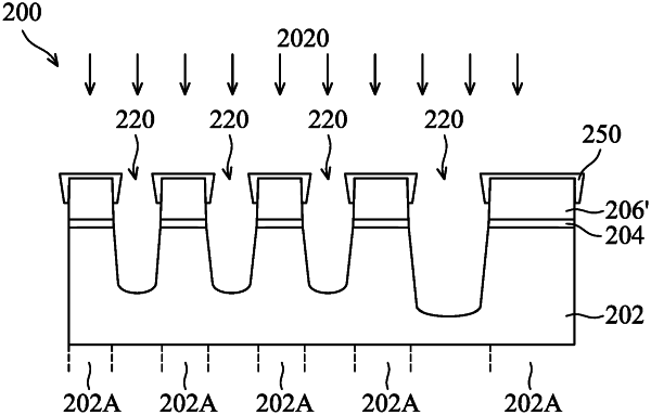
1. A method for forming a semiconductor structure, comprising:
providing a semiconductor substrate;
forming a sacrificial layer over the semiconductor substrate;
etching the sacrificial layer to form a sacrificial pattern, wherein etching the sacrificial layer comprises introducing an etching gas and a passivation gas in a first step, wherein a ratio of a flow rate of the etching gas to a flow rate of the passivation gas in the first step is a first ratio;
etching the semiconductor substrate using the sacrificial pattern as an etching mask to form an active region of the semiconductor substrate;
trimming the sacrificial pattern, comprising introducing the etching gas and the passivation gas in a second step, wherein a ratio of a flow rate of the etching gas to a flow rate of the passivation gas in the second step is a second ratio, wherein the second ratio is less than the first ratio; and
replacing the trimmed sacrificial pattern with a gate electrode.
|